 ALLPCB
Mastering High Speed PCB Layout: Techniques for SI and EMC
Master high-speed PCB layout with techniques for signal integrity, EMC compliance, controlled impedance, crosstalk reduction, and grounding.



Master high-speed PCB layout with techniques for signal integrity, EMC compliance, controlled impedance, crosstalk reduction, and grounding.

Explore the challenges of miniaturization and power efficiency in integrated circuits for wearable tech, with solutions for IC design and PCB innovation.

Learn best practices for through-hole PCB design reliability. Discover tips for robust through-hole design and build a reliable PCB with ALLPCB.

Discover fast, efficient RF PCB prototyping techniques with ALLPCB. Learn about quick-turn services, assembly, costs, and testing for your designs.

Explore if standard PCB dimensions exist in power electronics. Learn key factors, common sizes, and design tips for optimal layouts.
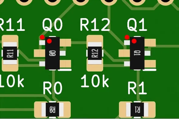
Learn PCB component placement strategies to maximize performance and reduce noise. Explore tips for high-speed designs and orientation.
Learn hobbyists! Discover easy-to-use PCB schematic tools and free design software for beginners to kickstart your electronics journey.
Learn essential PCB grounding techniques for high-power boards to ensure reliable, safe electronic designs with minimal noise and EMI.

Explore top PCB design software for flexible circuits, focusing on flex PCB layout, rigid-flex design, bend radius tools, and material selection.

Learn through-hole grounding and power distribution for PCBs. Optimize designs with ground planes and practical tips for reliability.