Attentions in PCB Copper Cladding
Copper cladding is an essential part of PCB design. Copper cladding is to take the unused space on the PCB board as a
reference and fill with solid copper, which aims to enhance the anti-resistance
capacity, improve the power efficiency and reduce the loop area.
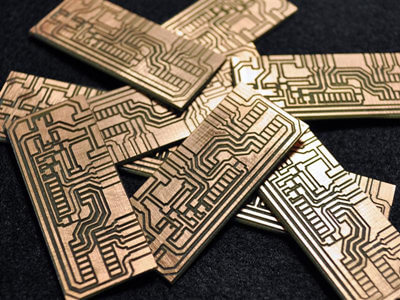
PCB Copper Cladding
And here are some attentions to achieve the
expected result of copper cladding:
1. If there are several grounds like SGND,
AGND and GND, it is necessary to conduct different treatment according to the
position. Besides, it is better to bold the power connection relatively, to
form a plurality of multi-deformable in different shape.
2. For the single point connection of different
grounds, the best option is to connect by 0 ohm resistor, inductor or magnetic
beads.
3. The cladding copper around crystal
oscillator is to take the crystal oscillator as the high frequency emission
source and then clad the copper around crystal oscillator that separately
grounded.
4. At the beginning of layout, grounding
should be given equal attentions. It is better to make an excellent layout
instead of relying on vias to eliminate the ground pin, which is a good choice
for PCB manufacture.
5. No sharp corner should be allowed on PCB
board. From the perspective of electromagnetic, a corner on PCB board means a
transmitting antenna that will influence the circuit in the future. So you’d
better to apply rounding edge.
6. Do not clad copper on the spare layout
area of multilayer for the difficulty in good ground of the cladding copper.
7. To achieve the good grounding about the
inner metal, like metal radiator and metal reinforcement, etc.
8. The radiation metal of three-terminal
voltage regulator must be well grounded. And the grounding isolation zone must
be well grounded.
In short, if the ground of cladding copper on PCB is well treated, it definitely brings more good than harm. It can reduce
the reflux area of signal line and reduce external electromagnetic interference
for signal.


