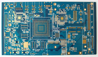


● 2 Kinds of 8 Layer PCB Stackup
● 8 Layer PCB Stackup Guidelines
Instant Quote
Full feature prototype PCB custom service at low cost.
Flexible PCB
Customized FPC service with high standards
Rigid-Flex PCB
High precision rigid-flex PCB customized service
PCB Assembly Quote
Leading assembly factory with Siemens production line
SMD-Stencil
Laser cutting high precision stencil service
The 8 Layer PCB stack-up offers ample routing space for multiple power islands. All signal layers have a minimum of one referencing power plane. The power and ground layer in the center offers good inter plane capacitance. If your system has a lot of power islands and these power islands are near to the bottom layer, they have no enough power to ground capacitance. Besides, the return path for the high speed signals in bottom layer (signal4) refer to the power plane, which isn’t adjacent to a ground plane.
8 Layer PCB Stackup

8 layer PCB is stacked together firmly with dependable and predefined mutual connections between all the layers. In order to ensure the quality, a complex manufacturing process is needed. By keeping the separation between signal2 and signal3 giant, we are able to eliminate any potential crosstalk between signal2 and signal3.
A typical 8 Layer PCB Stackup:
Signal1 - Ground - Signal2 - Power- Ground - Signal3 - Power - Signal4
An alternative 8 Layer PCB Stackup:
Signal1 - Ground - Power- Signal2 - Signal3 - Ground - Power - Signal4
8 Layer PCB Stackup Guidelines in 2018
An 8 layer PCB board can be used to add two more routing layers or to enhance EMC performance by adding two more planes. Though we may see examples of each case, however, the majority of 8 layer PCB board stack-ups are used to improve EMC performance instead of adding further routing layers. The percentage increase in cost of an 8 layer PCB board over a 6 layer PCB board is less than the percentage increase in going from 4 layer PCB to, therefore, making it easier to justify the cost increase for improved EMC performance.


An 8 layer PCB offers us the chance to simply satisfy all of the 5 originally declared objectives. Though many other stack-ups are also possible, we are going to solely discuss a few of them that have proven themselves by providing brilliant EMC performance. 8 layer PCB is sometimes used to improve the EMC performance of the board, not to increase the quantity of routing layers.
An 8 layer PCB board with 6 routing layers is unquestionably not recommended, no matter how you decide to stack-up the layers. If you need 6 routing layers you should use a 10 layer PCB board. Therefore, an 8 layer PCB board can be thought of as a 8 layer PCB board with optimum EMC performance.
Two plane layers are added to the centre of the substrate. This enables tight coupling between the centre planes and isolates every signal plane reducing coupling hence crosstalk dramatically. This configuration is usually used for high speed signals of DDR2 and DDR3 designs where crosstalk due to tight routing is a difficulty.
Why do you need an experienced 8 layers PCB manufacturer?
8 layer PCB board is widely used in compact devices, which require restrict spacing. Because of its complexity and high cost, your 8 layers PCB ought to be fabricated by an experienced and professional PCB manufacturer.
ALLPCB has manufacturing and assembly services for 8 layer PCB circuit board for over 10 years. Over 30,000 customers around the world have proved the good quality and outstanding services. Our advanced production lines, online PCB ordering system and customer service team make it come true, that you can complete your PCB order online, easily and quickly.


Terms of Service | Privacy Policy | Refund Policy | Sitemap
© ALLPCB.com, All Rights Reserved


